
Breakthrough in materials science: AI reveals secrets of dendritic growth in thin films
Thin film devices, composed of layers of materials a few nanometers thick, play an important role in various technologies, from semiconductors to communication technologies. For instance, graphene and hexagonal-boron nitride (h-BN) multilayer thin films, deposited on copper substrates, are promising materials for next-generation high-speed communications systems. Thin films are grown by depositing tiny layers of materials onto a substrate. The growth process conditions significantly influence the microstructure of these films, which in turn influences their function and performance.
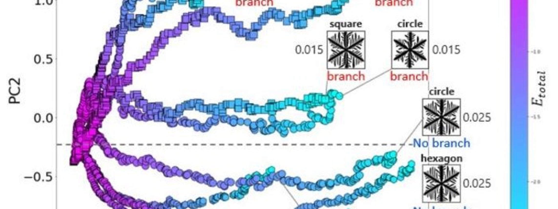
Dendritic structures, or tree-like branching patterns that emerge during growth, pose a major challenge to large-area fabrication of thin-film devices, a key step toward commercial application. They are commonly observed in materials like copper, graphene, and borophene, particularly in the early growth stage and multilayer films. Since the microstructure directly impacts device performance, reducing dendritic formation is, therefore, critical. However, methods for studying dendrites have largely relied on crude visual analysis and subjective interpretation. Understanding the conditions that drive dendritic branching is essential for optimizing the thin-film growth process, but existing approaches often require considerable trial and error.